Categories: Featured Articles » Novice electricians
Number of views: 36288
Comments on the article: 3
Transistors Part 3. What transistors are made of
Beginning of the article: Transistor history, Transistors: purpose, device and principles of operation, Conductors, Insulators and Semiconductors
 Pure semiconductors have the same amount of free electrons and holes. Such semiconductors are not used for the manufacture of semiconductor devices, as was said in the previous part of the article.
For the production of transistors (in this case, they also mean diodes, microcircuits, and actually all semiconductor devices), n and p types of semiconductors are used: with electronic and hole conductivity. In n-type semiconductors, electrons are the main charge carriers, and holes in p-type semiconductors.
Semiconductors with the required type of conductivity are obtained by doping (adding impurities) to pure semiconductors. The amount of these impurities is small, but the properties of the semiconductor change beyond recognition.
Dopants
Transistors would not be transistors if they did not use three and pentavalent elements, which are used as alloying impurities. Without these elements, it would simply have been impossible to create semiconductors of different conductivity, to create a pn (reads pe - en) junction and transistor as a whole.
On the one hand, indium, gallium, and aluminum are used as trivalent impurities. Their outer shell contains only 3 electrons. Such impurities take away electrons from the atoms of the semiconductor, with the result that the conductivity of the semiconductor becomes hole. Such elements are called acceptors - "taker."
On the other hand, these are antimony and arsenic, which are pentavalent elements. They have 5 electrons in their outer orbit. Entering the orderly rows of the crystal lattice, they cannot find a place for the fifth electron, it remains free, and the conductivity of the semiconductor becomes electron or type n. Such impurities are called donors - the “giver”.
Figure 1 shows a table of chemical elements that are used in the production of transistors.

Figure 1. The effect of impurities on the properties of semiconductors
Even in a chemically pure crystal of a semiconductor, for example, germanium, impurities are contained. Their number is small - one impurity atom per one billion atoms of Germany itself. And in one cubic centimeter it turns out about fifty thousand billion foreign bodies, which are called impurity atoms. Like a lot?
Here is the time to remember that at a current of 1 A, a charge of 1 Coulomb, or 6 * 10 ^ 18 (six billion billion) electrons per second, passes through the conductor. In other words, there are not so many impurity atoms and they give the semiconductor very little conductivity. It turns out either a bad conductor, or not a very good insulator. In general, a semiconductor.
How is a semiconductor with a conductivity n
Let's see what happens if a pentavalent atom of antimony or arsenic is introduced into a germanium crystal. This is shown quite clearly in Figure 2.

Figure 2. Introduction of a 5-valence impurity into a semiconductor.
A short commentary on Figure 2, which should have been done earlier. Each line between adjacent atoms of the semiconductor in the figure should be double, showing that two electrons are involved in the bond. Such a bond is called covalent and is shown in Figure 3.

Figure 3. Covalent bond in a silicon crystal.
For Germany, the pattern would be exactly the same.
A pentavalent impurity atom is introduced into the crystal lattice, because it simply has nowhere to go.He uses four of his five valence electrons to create covalent bonds with neighboring atoms, and is introduced into the crystal lattice. But the fifth electron will remain free. The most interesting thing is that the atom of the impurity itself in this case becomes a positive ion.
The impurity in this case is called a donor; it gives the semiconductor additional electrons, which will be the main charge carriers in the semiconductor. The semiconductor itself, which received additional electrons from the donor, will be a semiconductor with electronic conductivity or of type n - negative.
Impurities are introduced into semiconductors in small quantities, only one atom per ten million atoms of germanium or silicon. But this is a hundred-odd times more than the content of intrinsic impurities in the purest crystal, as was written just above.
If we now attach a galvanic cell to the resulting type n semiconductor, as shown in Figure 4, then the electrons (circles with a minus inside) under the action of the electric field of the battery will rush to its positive output. The negative pole of the current source will give as many electrons to the crystal. Therefore, an electric current will flow through the semiconductor.
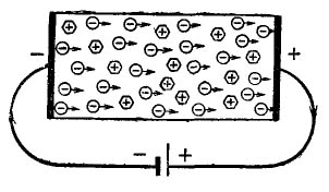
Figure 4
Hexagons, which have a plus sign inside, are nothing but impurity atoms that donate electrons. Now these are positive ions. The result of the foregoing is as follows: the introduction of an impurity donor into the semiconductor ensures the injection of free electrons. The result is a semiconductor with electronic conductivity or type n.
If atoms of a substance with three electrons in an external orbit, such as indium, are added to a semiconductor, germanium or silicon, then the result will, quite frankly, be the opposite. This association is shown in Figure 5.

Figure 5. Introduction of a 3-valence impurity into a semiconductor.
If a current source is now attached to such a crystal, then the movement of holes will take an ordered character. Displacement phases are shown in Figure 6.

Figure 6. Hole conduction phases
The hole located in the first atom on the right, this is just the trivalent impurity atom, captures the electron from the neighbor on the left, as a result of which the hole remains in it. This hole, in turn, is filled with an electron torn from its neighbor (in the figure it is again to the left).
In this way, the movement of positively charged holes from the positive to the negative pole of the battery is created. This continues until the hole comes close to the negative pole of the current source and is filled with an electron from it. At the same time, the electron leaves its atom from the source closest to the positive terminal, a new hole is obtained, and the process is repeated again.
In order not to get confused about what type of semiconductor is obtained when an impurity is introduced, it is enough to remember that the word “donor” has the letter en (negative) - a semiconductor of type n is obtained. And in the word acceptor there is the letter pe (positive) - a semiconductor with conductivity p.
Conventional crystals, for example, Germany, in the form in which they exist in nature, are unsuitable for the production of semiconductor devices. The fact is that an ordinary natural germanium crystal consists of small crystals grown together.
First, the starting material was purified from impurities, after which germanium was melted and a seed was lowered into the melt, a small crystal with a regular lattice. The seed slowly rotated in the melt and gradually rose up. The melt enveloped the seed and cooling formed a large single crystal rod with a regular crystal lattice. The appearance of the obtained single crystal is shown in Figure 7.
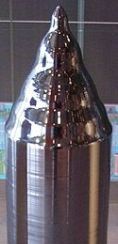
Figure 7
In the process of manufacturing a single crystal, a dopant of p or n type was added to the melt, thereby obtaining the desired conductivity of the crystal. This crystal was cut into small plates, which in the transistor became the base.
The collector and emitter were made in different ways. The simplest was that small pieces of indium were placed on opposite sides of the plate, which were welded, warming the contact point to 600 degrees. After cooling of the entire structure, the indium-saturated regions acquired p type conductivity. The obtained crystal was installed in the housing and the leads were connected, as a result of which alloyed planar transistors were obtained. The design of this transistor is shown in Figure 8.
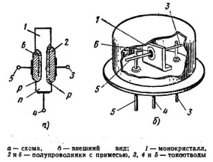
Figure 8
Such transistors were produced in the sixties of the twentieth century under the brand name MP39, MP40, MP42, etc. Now it is almost a museum exhibit. The most widely used transistors of the p-n-p circuit structure.
In 1955, a diffusion transistor was developed. According to this technology, to form the collector and emitter regions, a germanium plate was placed in a gas atmosphere containing vapors of the desired impurity. In this atmosphere, the plate was heated to a temperature just below the melting point and held for the required time. As a result, impurity atoms penetrated the crystal lattice, forming pn junctions. Such a process is known as the diffusion method, and the transistors themselves are called diffusion.
The frequency properties of alloy transistors, it must be said, leave much to be desired: the cutoff frequency is not more than several tens of megahertz, which allows you to use them as a key at low and medium frequencies. Such transistors are called low-frequency, and will confidently amplify only the frequencies of the audio range. Although silicon alloy transistors have long been replaced by silicon transistors, germanium transistors are still being manufactured for special applications where low voltage is required to bias the emitter in the forward direction.
Silicon transistors are produced according to planar technology. This means that all transitions go to one surface. They almost completely replaced germanium transistors from discrete element circuits and are used as components of integrated circuits where germanium has never been used. Currently, a germanium transistor is very difficult to find.
Read on in the next article.
Boris Aladyshkin
See also at e.imadeself.com
: