Categories: Featured Articles » Novice electricians
Number of views: 83382
Comments on the article: 0
Characteristics of Bipolar Transistors
 At the very end of the previous part of the article, a “discovery” was made. Its meaning is that a small base current controls a large collector current. This is precisely the main property. transistor, its ability to amplify electrical signals. In order to continue the further narration, it is necessary to understand how large the difference of these currents is, and how this control occurs.
To better remember what is being said, Figure 1 shows an n-p-n transistor with power supplies for the base and collector circuits connected to it. This drawing has already been shown. in the previous part of the article.
A small remark: everything that is told about the transistor of the n-p-n structure is quite true for the p-n-p transistor. Only in this case should the polarity of the power sources be reversed. And in the description itself, “electrons” should be replaced with “holes”, wherever they occur. But at present, transistors of the n-p-n structure are more modern, more in demand, therefore, it is mainly about them that are told.

Picture 1.
Low power transistor. Voltages and currents
The voltage applied to the emitter junction (as the base-emitter junction is commonly called) is low for low-power transistors, not more than 0.2 ... 0.7V, which allows creating a current of several tens of microamps in the base circuit. Base current versus base voltage - emitter is called transistor input characteristic, which is removed at a fixed collector voltage.
A voltage of the order of 5 ... 10 V is applied to the collector junction of a low-power transistor (this is for our research), although it can be more. At such voltages, the collector current can be from 0.5 to several tens of milliamps. Well, just within the framework of the article we will restrict ourselves to such quantities, since it is believed that the transistor is low-power.
Transmission characteristics
As mentioned above, a small base current controls a large collector current, as shown in Figure 2. It should be noted that the base current on the graph is indicated in microamps, and the collector current in milliamps.

Figure 2
If you carefully monitor the behavior of the curve, you can see that for all points in the graph the ratio of the collector current to the base current is the same. To do this, it is enough to pay attention to points A and B, for which the ratio of the collector current to the base current is exactly 50. This will be the CURRENT ACCELERATION, indicated by the symbol h21e - current gain.
h21e = Ik / Ib.
Knowing this ratio, it is not difficult to calculate the collector current Ik = Ib * h21e
But in no case should you think that the gain of all transistors is exactly 50, as in Figure 2. In fact, depending on the type of transistor, it ranges from units to several hundred and even thousands!
If you need to know the gain for a specific transistor that lies on your table, then this is quite simple: modern multimeters, as a rule, have a measurement mode of h21e. Next, we will explain how to determine the gain using a conventional ammeter.
The dependence of the collector current on the base current (Figure 2) is called transistor response. Figure 3 shows a family of transfer characteristics of a transistor when it is turned on according to a circuit with OE. Characteristics are taken at a fixed collector-emitter voltage.

Figure 3. The family of transfer characteristics of the transistor, when it is turned on according to the scheme with OE
If you look at this family more closely, you can draw several conclusions.Firstly, the transfer characteristic is non-linear, it is a curve (although there is a linear section in the middle of the curve). It is this curve that leads to nonlinear distortions if the transistor is used to amplify a signal, for example, an audio one. Therefore, it is necessary to “shift” the operating point of the transistor to a linear portion of the characteristic.
Secondly, the characteristics taken at different voltages Uke1 and Uke2 are equidistant (equidistant from each other). This allows us to conclude that the gain of the transistor (determined by the angle of the curve to the coordinate axis) does not depend on the collector-emitter voltage.
Thirdly, characteristics do not start at the origin. This suggests that even at zero base current, some current flows through the collector. This is exactly the initial current, which was described in the previous part of the article. The initial current for both curves is different, which indicates that it depends on the voltage on the collector.
How to remove the transfer characteristic
The easiest way to remove this characteristic is if you turn on the transistor according to the circuit shown in Figure 4.
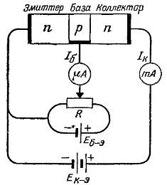
Figure 4
By turning the knob of the potentiometer R, you can change a very small base current Ib, which will lead to a proportional change in the large collector current Ik. Such a “creative” process as the rotation of the knob of a potentiometer involuntarily suggests: “Is it possible to automate this process of torsion of a knob somehow?” It turns out you can.
To do this, instead of a potentiometer, it is enough to connect an alternating voltage source, for example, a carbon microphone, an oscillatory circuit of an antenna or a detector of a receiver, from the EB-e batteries in series. Then this alternating voltage will control the collector current of the transistor, as shown in Figure 5.
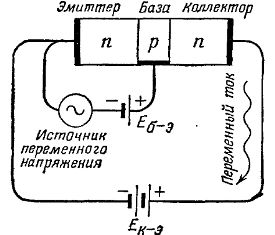
Figure 5
In this circuit, the EB-e battery acts as a bias source for the operating point of the transistor, and the AC voltage signal will be amplified. If you apply an alternating signal, for example a sinusoid, without bias, then the positive half-cycles will open the transistor, and possibly even amplify.
But the negative half-periods the transistor is simply closed, so not only will not amplify, but even will not pass through the transistor. It’s about the same as if you connect the loudspeaker through a diode: instead of pleasant music and voices, you can hear incomprehensible wheezing.
But quite often they amplify direct current, while the transistor works in a key mode, like a relay. This application is most often found in digital circuits. In the next article, it is with the key mode, as the simplest and most understandable, that we will begin to consider the various modes of operation of the transistor.
Transistor Switching Circuits

Figure 6. Transistor switching circuits
Until now, in all the figures, the transistor appeared before us as three squares with the letters n and p. In Figure 6a, the transistor is shown as in a real electrical circuit. The polarity of the voltage connection, the names of the electrodes, the base and emitter currents are immediately shown. And in Figure 6b, in the form of a design of two diodes, which is often used when testing a transistor with a multimeter.
See also at e.imadeself.com
: